IMAGE BEST3D Wafer Stacking: Review paper in IEEE TED June 2022 IssueAMMJENACIONAL
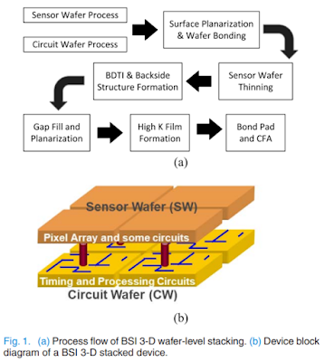
In IEEE Trans. Electr. Dev. June 2022 issue, in a paper titled "A Review of 3-Dimensional Wafer Level Stacked Backside Illuminated CMOS Image Sensor Process Technologies," Wuu et al. write: Over the past 10 years, 3-dimensional (3-D) wafer-level stacked backside Illuminated (BSI) CMOS image sensors (CISs) have undergone rapid progress in development and performance and are now in mass production. This review paper covers the key processes and technology components of 3-D integrated BSI devices, as well as results from early devices fabricated and tested in 2007 and 2008. This article is divided into three main sections. Section II covers wafer-level bonding technology. Section III covers the key wafer fabrication process modules for BSI 3-D waferlevel stacking. Section IV presents the device results. This paper has quite a long list of acronyms. Here is a quick reference: BDTI = backside deep trench isolation BSI = backside illumination BEOL = back end of line HB = hybrid bon...