Postingan

Menampilkan postingan dari Juli, 2022

IMAGE BESTSigma Foveon sensor will be ready in 2022AMMJENACIONAL

Gambar
From PetaPixel : Sigma’s CEO Kazuto Yamaki has revealed that the company’s efforts in making a full-frame Foveon sensor are on track to be finished by the end of the year.  Sigma’s Foveon sensors use a proprietary three-layer structure in which red, green, and blue pixels each have their own full layer. In traditional sensors, the three pixels share a single layer in a mosaic arrangement and the camera “fills in” missing colors by examining neighboring pixels. Since each pixel of a photo is recorded in three colors, the resulting photo should be sharper with better color accuracy and fewer artifacts. The release had been delayed on at least two occasions in the past due to technical challenges, once in 2020 and again in 2021. The initial announcement about this sensor was made back in 2018. In February 2022, Yamaki indicated that the company was in stage 2 of testing, and the final third stage will involve mass-production testing.
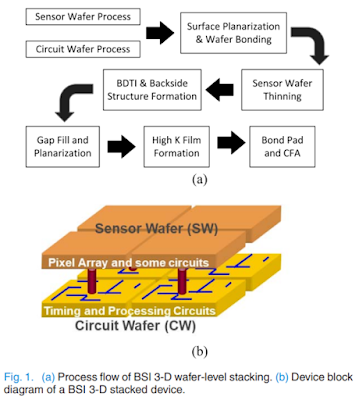
IMAGE BESTProphesee interview in EETimes AMMJENACIONAL

Gambar
EETimes has published an interview with CEO of Prophesee about their event sensor technology. Some excerpts below.   Prophesee collaborated with Sony on creating the IMX636 event sensor chip.   Meaning of "neuromorphic" Most companies doing neuromorphic sensing and computing have a similar vision in mind, but implementations and strategies will be different based on varying product, market, and investment constraints. ... ... there is a fundamental belief that the biological model has superior characteristics compared to the conventional ... Markets targeted ... the sector closest to commercial adoption of this technology is industrial machine vision. ... The second key market for the IMX 636 is consumer technologies, ... the event–based camera is used alongside a full–frame camera, detecting motion ... correct any blur. Prophesee is also working with a customer on automotive driver monitoring solutions... Applications here include eye blinking detection, tracking or face tr

IMAGE BEST3D cameras for metaverseAMMJENACIONAL

Gambar
Press release from II-VI Inc. announces joint effort with Artilux on a SWIR 3D camera for the "metaverse". https://ii-vi.com/news/ii-vi-incorporated-and-artilux-demonstrate-a-3d-camera-for-enhanced-user-experience-in-the-metaverse/   PITTSBURGH and HSINCHU, TAIWAN, July 18, 2022 (GLOBE NEWSWIRE) – II‐VI Incorporated (Nasdaq: IIVI), a leader in semiconductor lasers, and Artilux, a leader in germanium silicon (GeSi) photonics and CMOS SWIR sensing technology, today announced a joint demonstration of a next-generation 3D camera with much longer range and higher image resolution to greatly enhance user experience in the metaverse. Investments in the metaverse infrastructure are accelerating and driving the demand for sensors that enable more realistic and immersive virtual experiences. II-VI and Artilux combined their proprietary technologies in indium phosphide (InP) semiconductor lasers and GeSi sensor arrays, respectively, to demonstrate a miniature 3D camera that operates in

IMAGE BESTReview of indirect time-of-flight 3D cameras (IEEE TED June 2022)AMMJENACIONAL

Gambar
C. Bamji et al. from Microsoft published a paper titled "A Review of Indirect Time-of-Flight Technologies" in IEEE Trans. Electron Devices (June 2022). Abstract: Indirect time-of-flight (iToF) cameras operate by illuminating a scene with modulated light and inferring depth at each pixel by combining the back-reflected light with different gating signals. This article focuses on amplitude-modulated continuous-wave (AMCW) time-of-flight (ToF), which, because of its robustness and stability properties, is the most common form of iToF. The figures of merit that drive iToF performance are explained and plotted, and system parameters that drive a camera’s final performance are summarized. Different iToF pixel and chip architectures are compared and the basic phasor methods for extracting depth from the pixel output values are explained. The evolution of pixel size is discussed, showing performance improvement over time. Depth pipelines, which play a key role in filtering and enhanc

IMAGE BESTAmphibious panoramic bio-inspired camera in Nature ElectronicsAMMJENACIONAL

Gambar
M. Lee at al. have published a paper titled "An amphibious artificial vision system with a panoramic visual field" in Nature Electronics. This paper is joint work between researchers in Korea (Institute of Basic Science, Seoul National University, Pusan National University) and USA (UT Austin and MIT). Abstract: Biological visual systems have inspired the development of various artificial visual systems including those based on human eyes (terrestrial environment), insect eyes (terrestrial environment) and fish eyes (aquatic environment). However, attempts to develop systems for both terrestrial and aquatic environments remain limited, and bioinspired electronic eyes are restricted in their maximum field of view to a hemispherical field of view (around 180°). Here we report the development of an amphibious artificial vision system with a panoramic visual field inspired by the functional and anatomical structure of the compound eyes of a fiddler crab. We integrate a microlens

IMAGE BESTIEEE International Conference on Computational Photography 2022 in Pasadena (Aug 1-3)AMMJENACIONAL

Gambar
[Jul 16, 2022] Update from program chair Prof. Ioannis Gkioulekas: All paper presentations will be live-streamed on the ICCP YouTube channel: https://www.youtube.com/channel/UClptqae8N3up_bdSMzlY7eA You can watch them for free, no registration required. You can also use the live stream to ask the presenting author questions. ICCP will take place in person in Caltech (Pasadena, CA) from August 1 to 3, 2022. The final program is now available here:  https://iccp2022.iccp-conference.org/program/ There will be an exciting line up of: three keynote speakers, Shree Nayar, Changhuei Yang, Joyce Farrell; ten invited speakers, spanning areas from acousto-optics and optical computing, to space exploration and environment conservation; and  24 paper and more than 80 poster and demo presentations.  Registration page:  https://www.eventbee.com/v/ieee-international-conference-on-computational-photography-iccp-2022/event?eid=285801623 List of accepted papers with oral presentations: #16: Learning Spa

IMAGE BESTDetailed depth maps from gated camerasAMMJENACIONAL

Gambar
Recent work from Princeton University's computational imaging lab shows a new method for generating highly detailed depth maps from a gated camera.  This work was presented at the recent IEEE/CVF Computer Vision and Pattern Recognition 2022 conference in New Orleans. Abstract:  Gated cameras hold promise as an alternative to scanning LiDAR sensors with high-resolution 3D depth that is robust to back-scatter in fog, snow, and rain. Instead of sequentially scanning a scene and directly recording depth via the photon time-of-flight, as in pulsed LiDAR sensors, gated imagers encode depth in the relative intensity of a handful of gated slices, captured at megapixel resolution. Although existing methods have shown that it is possible to decode high-resolution depth from such measurements, these methods require synchronized and calibrated LiDAR to supervise the gated depth decoder – prohibiting fast adoption across geographies, training on large unpaired datasets, and exploring alternativ

IMAGE BEST3D Wafer Stacking: Review paper in IEEE TED June 2022 IssueAMMJENACIONAL

Gambar
In IEEE Trans. Electr. Dev. June 2022 issue, in a paper titled "A Review of 3-Dimensional Wafer Level Stacked Backside Illuminated CMOS Image Sensor Process Technologies," Wuu et al. write: Over the past 10 years, 3-dimensional (3-D) wafer-level stacked backside Illuminated (BSI) CMOS image sensors (CISs) have undergone rapid progress in development and performance and are now in mass production. This review paper covers the key processes and technology components of 3-D integrated BSI devices, as well as results from early devices fabricated and tested in 2007 and 2008. This article is divided into three main sections. Section II covers wafer-level bonding technology. Section III covers the key wafer fabrication process modules for BSI 3-D waferlevel stacking. Section IV presents the device results. This paper has quite a long list of acronyms. Here is a quick reference: BDTI = backside deep trench isolation BSI = backside illumination BEOL = back end of line HB = hybrid bon

IMAGE BESTXiaomi 12s will have a 1" sensorAMMJENACIONAL

Gambar
From PetaPixel : Xiaomi has announced that it’s upcoming 12S Ultra will use the full size of Sony’s IMX989 1-inch sensor. The phone, which is also co-developed with Leica, will be announced on July 4.   Xiaomi’s Lei Jun says that the 1-inch sensor that is coming to the 12S Ultra, crucially, won’t be cropped. How the company plans to deal with physical issues Sony came up against in its phone isn’t clear. Jun also says that Xiaomi didn’t just buy the sensor, but that it was co-developed between the two companies with a total investment cost of $15 million split evenly between them. The fruits of this development will first come to the 12S Ultra before being made available to other smartphone manufacturers, so it’s not exclusive to Xiaomi forever. ... o nly the 12S Ultra will feature a 1-inch sensor while the 12S and 12S Pro will feature the Sony IMX707 instead.  

IMAGE BESTHigh resolution ToF module from Analog DevicesAMMJENACIONAL

Gambar
Analog Devices has released an industrial-grade megapixel ToF module ADTF3175 and a VGA resolution sensor the ADSD3030 that seeks to bring the highest accuracy ToF technology in the most compact VGA footprint. ADTF3175 Features The ADTF3175 is a complete Time-of-Flight (ToF) module for high resolution 3D depth sensing and vision systems. Based on the ADSD3100, a 1 Megapixel CMOS indirect Time-of-Flight (iToF) imager, the ADTF3175 also integrates the lens and optical bandpass filter for the imager, an infrared illumination source containing optics, laser diode, laser diode driver and photodetector, a flash memory, and power regulators to generate local supply voltages. The module is fully calibrated at multiple range and resolution modes. To complete the depth sensing system, the raw image data from the ADTF3175 is processed externally by the host system processor or depth ISP. The ADTF3175 image data output interfaces electrically to the host system over a 4-lane mobile industry proce

IMAGE BESTLabforge releases new 20.5T ops/s AI machine vision cameraAMMJENACIONAL

Gambar
Labforge has designed and developed a smart camera called Bottlenose which supports 20.5 trillion operations/second processing power and on-board AI, depth, feature points & matching, and a powerful ISP. The target audience is robotics and automation. They have built the camera around a Toshiba Visconti-5 processor. The current models are available as both stereo and monocular versions with IMX577 Sony image sensors. For future models there will be a range of resolutions and shutter options available.  Datasheet:  labforge.ca/wp-content/ uploads/2022/05/Labforge- Bottlenose-Datasheet-0.84.pdf Labforge has announced a distribution agreement with Mouser Electronics:   mouser.ca/newsroom/ publicrelations-labforge-new- manufacturer-2022final/

IMAGE BESTSony releases new sensors IMX487, IMX661AMMJENACIONAL

Gambar
IMX487 UV 8.13MP [Advertised as "new product launch" but this has been around for a while.] Global shutter CMOS image sensor specialized for the UV spectrum With the structure specially designed for the properties of the UV wavelengths coupled with Pregius S technology, the image sensor can capture undistorted images of moving objects within a UV range of 200–400 nm and at a high frame rate of 193 fps (operated in the 10-bit mode). This image sensor has a potential to expand the scope of application from the conventional use of UV cameras in the inspection of semiconductors, etc. to areas that require high-speed capability, such as sorting of recycled materials. Low noise This image sensor has adopted the component materials dedicated for UV range imaging, and a special structure has been developed for its light receiving area. These make it possible to maintain high UV sensitivity while significantly minimizing noises to produce high quality images. Smaller pixels The pixels

IMAGE BESTSamsung's ISOCELL HP3 sensorAMMJENACIONAL

Gambar
Samsung has published details about its now 200MP sensor 'ISOCELL HP3'. https://semiconductor.samsung.com/image-sensor/mobile-image-sensor/isocell-hp3/ Press release: https://news.samsung.com/global/samsung-unveils-isocell-image-sensor-with-industrys-smallest-0-56%CE%BCm-pixel Samsung Electronics, a world leader in advanced semiconductor technology, today introduced the 200MP ISOCELL HP3, the image sensor with the industry’s smallest 0.56-micrometer (μm)-pixels. “Samsung has continuously led the image sensor market trend through its technology leadership in high resolution sensors with the smallest pixels,” said JoonSeo Yim, Executive Vice President of Sensor Business Team at Samsung Electronics. “With our latest and upgraded 0.56μm 200MP ISOCELL HP3, Samsung will push on to deliver epic resolutions beyond professional levels for smartphone camera users.” Epic Resolution Beyond Pro Levels Since its first 108MP image sensor roll-out in 2019, Samsung has been leading the trend o